

Millikelvin-Level Precision Assurance, Crafting the Future with Core Technology—Application of Jice UPECS in Semiconductor Lithography
Release time:
2026-03-31
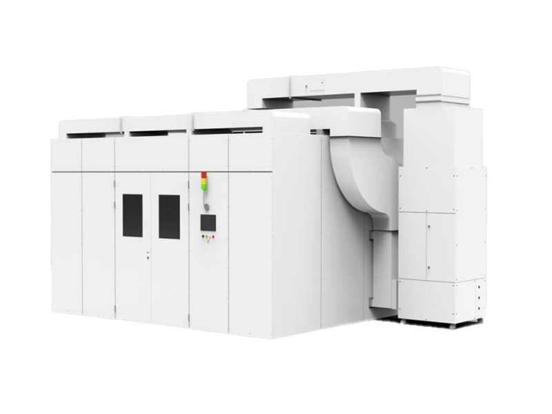
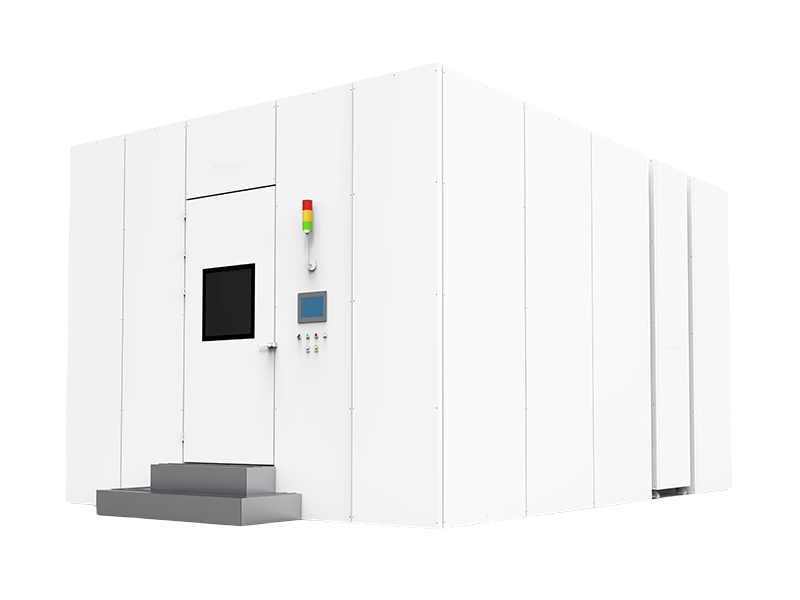
Jice’s UPECS modular design and custom non-standardization capabilities are tailored to meet the diverse requirements of lithography applications.
In the semiconductor chip manufacturing industry, the lithography process is often referred to as the “sculptor of chips,” as its precision directly determines chip performance and yield. As chip fabrication nodes advance to 3 nm and below, the operating environment for lithography equipment demands increasingly stringent standards for temperature, humidity, and cleanliness—standards that traditional environmental control systems can no longer adequately meet. This frequently results in unstable temperature control, delayed humidity regulation, and insufficient cleanliness, thereby becoming a bottleneck that hinders the mass production of high-end chips.
In response to the stringent requirements of lithography applications,
Extreme Testing UPECS Leveraging all-dimensional, precision control capabilities, UPECS breaks down industry-specific technical barriers and creates a stable, ultra-clean optimal operating environment for lithography equipment. In terms of temperature control, UPECS achieves air-temperature stability as tight as ±0.002°C (±2 mK), significantly surpassing the industry-standard ±0.01°C threshold, thanks to its proprietary high-precision temperature-control technology that enables rapid response and fine-tuned adjustments.
Humidity control and cleanliness assurance are also core strengths of UPECS. With humidity control accurate to ±0.1% RH and ISO Class 1 cleanliness, UPECS delivers a multi-parameter, synergistic precision environment that ensures the faithful replication of lithographic patterns.

In addition to unparalleled core performance, Jice UPECS’ modular design and custom non-standard configuration capabilities seamlessly accommodate the diverse requirements of lithography applications. By leveraging computational fluid dynamics (CFD) simulations to optimize airflow distribution, it effectively eliminates vortices and stagnant flow zones. Furthermore, for localized heat-generating areas on lithography equipment, dedicated local air-bath modules (ABMs) are deployed to create an “air curtain” that enables precise temperature control, ensuring overall environmental stability while delivering fine-grained regulation in specific regions. This solution is fully adaptable to the operational needs of various lithography processes and equipment models.
Jice UPECS has successfully served numerous global semiconductor leaders and national key laboratories, redefining the industry standard for high-precision environmental control.
Amid the wave of self-reliant development in the semiconductor industry, UPECS will continue to deepen its expertise in core applications such as lithography, relentlessly iterate its technologies, and strive toward ever-higher precision in environmental control, thereby providing precise support for chip manufacturing, helping China’s high-end semiconductor sector break through critical bottlenecks, and advancing into a new stage of higher-quality growth.
UAC300 High-Precision Environmental Control System

UBA300 High-Precision Environmental Control System

UAA300 High-Precision Environmental Control System
UCB100 High-Precision Environmental Control System

UCC100 High-Precision Environmental Control System

UCC100 High-Precision Environmental Control System

UBA200 High-Precision Silent Environmental Control System
Here is the title one h1 placeholder text
More news

Service Hotline
E-mail:info@jicenj.com
Address: Block D, Tengfei Building, 88 Jiangmiao Road, Yanchuang Garden, Jiangbei New District, Nanjing City
Copyright © 2024 JICE(Nanjing) Technology Co., LTD