

Precision Environmental Control Applications of Jice UPECS in Semiconductor Scenarios
Release time:
2026-04-02
The UPECS system is leveraging its precise environmental control capabilities to help the semiconductor industry break through physical limits.
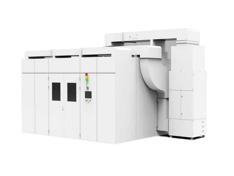
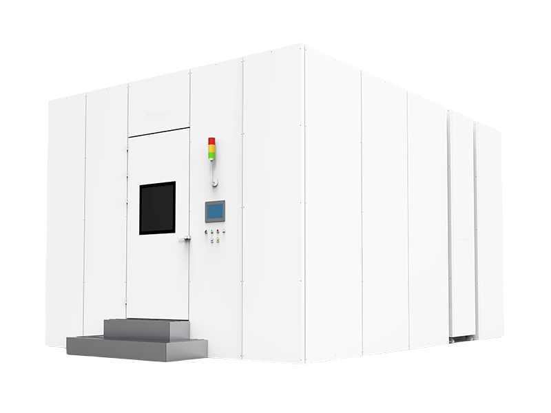
In the field of semiconductor manufacturing, Jice (Nanjing) Technology Co., Ltd. The newly launched high-precision environmental control system, UPECS, delivers temperature control stability of ±0.002°C, humidity control stability of ±0.1% RH, and ISO Class 1 cleanliness, making it a critical enabler for the stable operation of high-end equipment such as lithography tools, bonding equipment, and semiconductor metrology systems.
I. Lithography Process: Millikelvin-Level Temperature Control Ensures Nanometer-Scale Precision
As the “heart” of chip manufacturing, lithography equipment’s optical system is highly sensitive to temperature fluctuations. UPECS employs a closed-loop airflow circulation system combined with a high-precision PID control algorithm to maintain temperature stability within the work area to ±0.002°C, thereby significantly enhancing the overlay accuracy of multi-pattern exposure (MPC).
In addition, the UPECS system is equipped with a high-efficiency clean-air filtration system that achieves ISO Class 1 cleanliness (≤10 particles ≥0.1 μm per cubic meter), coupled with humidity control stability of ±0.1% RH, effectively preventing photoresist surface defects and lens fogging caused by dust adhesion.

II. Bonding Process: Multi-Parameter Synergy Breaks Through Boundaries
In the fields of 3D packaging and advanced packaging, the precision of bonding equipment directly determines the electrical performance and reliability of chips. Take flip-chip bonding as an example: a temperature deviation of just 0.1°C can lead to variations in the molten state of the solder balls, resulting in defects such as cold joints or bridging. The UPECS system achieves millikelvin-level temperature control, thereby reducing the variability in bond strength.
In response to the stringent cleanliness requirements of hybrid bonding, the UPECS system is equipped with a high-efficiency filtration system that achieves ISO Class 1 cleanliness, thereby improving yield in the bonding process.
III. Measurement Equipment: A Stable Environment Underpins Data Reliability
In the field of semiconductor metrology, environmental fluctuations are a critical factor affecting measurement repeatability. For example, in optical critical dimension (OCD) measurement equipment, a temperature change of just 0.5°C can lead to refractive-index deviations, resulting in line-width measurement errors exceeding 1 nm. The UPECS system leverages proprietary high-precision temperature-control technology to ensure the output accuracy of metrology equipment.
IV. Customization Capabilities: Adapting to Diverse Process Requirements
The complexity of semiconductor manufacturing environments demands highly flexible environmental control equipment. The UPECS system features a modular design, enabling non-standard customization to meet the specific requirements of various process steps.
From laboratory R&D to mass-production lines, and from logic chips to power devices, the UPECS system is leveraging its precise environmental-control capabilities to help the semiconductor industry push beyond physical limits. This “molecular-level” mastery of environmental parameters will serve as a critical infrastructure for driving innovation across the industry.
UAC300 High-Precision Environmental Control System
UBA300 High-Precision Environmental Control System

UAA300 High-Precision Environmental Control System
UCB100 High-Precision Environmental Control System

UCC100 High-Precision Environmental Control System

UCC100 High-Precision Environmental Control System

UBA200 High-Precision Silent Environmental Control System
Here is the title one h1 placeholder text
More news

Service Hotline
E-mail:info@jicenj.com
Address: Block D, Tengfei Building, 88 Jiangmiao Road, Yanchuang Garden, Jiangbei New District, Nanjing City
Copyright © 2024 JICE(Nanjing) Technology Co., LTD