

Bond‑dissolution‑based high‑precision environmental control: UPECS delivers a stable process environment for advanced packaging wafer dicing.
Release time:
2026-10-20
Bonding requires highly precise environmental control to stabilize the process and prevent stress, humidity, and particulate contamination from degrading wafer quality.
In wafer-level packaging, 2.5D/3D packaging, chiplet integration, and ultra-thin wafer processing, temporary bonding and debonding are critical steps that ensure the wafer can proceed with further processing without interruption. After the wafer is temporarily bonded to a carrier, the carrier facilitates subsequent processes such as thinning, backside processing, etching, deposition, and interconnect formation. Once these steps are completed, the wafer is safely separated from the carrier using methods like laser‑induced debonding, thermal‑slip debonding, mechanical peel‑off debonding, or wet‑chemical debonding.

Delamination is not simply “removing the wafer.” For ultra-thin wafers, glass carriers, temporary bonding adhesives, and high-precision delamination equipment, factors such as temperature, humidity, cleanliness, vibration, and localized airflow variations can all affect wafer warpage, interfacial stress, residual adhesive residues, separation uniformity, and subsequent surface quality. Therefore, both the delamination equipment itself and its surrounding process area must maintain a stable, clean environment that can be continuously controlled.
Why is high-precision environmental control necessary for bond release?
The first critical issue is thermal stress. Wafers, carrier substrates, and temporary bonding adhesives typically exhibit different coefficients of thermal expansion. When ambient temperatures fluctuate or when the temperature field within the equipment is non-uniform, the differential thermal expansion of these materials can give rise to additional stresses at the interface. For large‑diameter wafers and ultra‑thin wafers, such stresses may manifest as warpage, localized delamination, chipping, or even edge defects.
Take laser debonding as an example: the key parameters that must be kept stable are laser energy density, spot size, defocus amount, and scan trajectory. Variations in ambient temperature can induce thermal drift in the wafer, the stage, optical components, and the equipment structure, causing the actual point of laser‑induced energy deposition at the interface to shift and compromising bonding‑uniformity. In contrast, thermal‑slip debonding is sensitive to unstable environmental boundary conditions: if the adhesive layer softens unevenly, shear forces and the peel‑off process will fluctuate. For mechanical peel‑off debonding, it is crucial to carefully control vibration, warpage, and stress transmission during the peeling process, thereby preventing impact on ultra‑thin wafers.
The second issue concerns humidity and the interfacial condition of the materials. Temporary bonding adhesives, release layers, and wafer surfaces can be quite sensitive to changes in humidity. Even minor fluctuations in humidity can alter material moisture uptake, interfacial adhesion, chemical reactions, and the state of residual contaminants. In wet‑chemical debonding or solvent‑based processes, it is also essential to maintain a stable process environment by integrating local exhaust ventilation, process temperature control, air cleanliness, and minimizing the frequency of operator interventions.
The third issue is particulate and residual contamination. After debonding, wafers typically undergo additional processes such as cleaning, inspection, film application, dicing, re‑bonding, or other packaging steps. If particles, adhesive debris, or chemical residues are generated during debonding, they can compromise subsequent surface treatments and bonding quality. Therefore, the debonding cleanroom, the microenvironment of the debonding equipment, and the wafer transfer area must be designed with appropriate clean airflow management and robust contamination control to meet process requirements.
Applications of UPECS in Bond-Release Scenarios
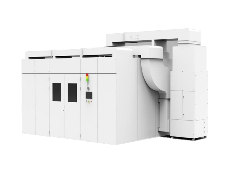
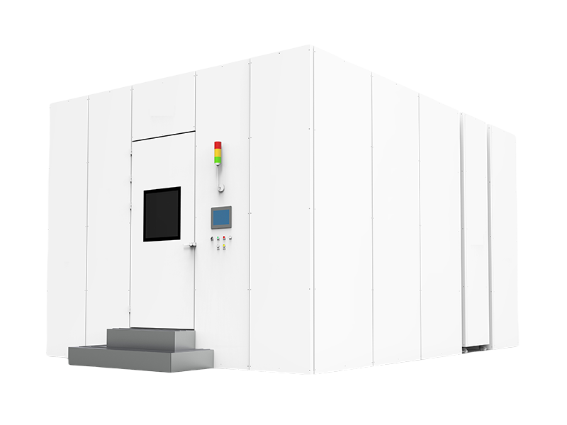
of Jice (Nanjing) Technology Co., Ltd. High-Precision Environmental Control System UPECS For precision manufacturing, advanced packaging, and highly stable process environments, we offer an integrated solution for the coordinated control of temperature, humidity, cleanliness, airflow distribution, and equipment interfaces, providing core environmental control subsystems and components to support a wide range of debonding equipment.
For different wire-bonding processes, UPECS’s core control capabilities can be optimized to achieve up to Temperature stability: ±0.002°C; humidity stability: ±0.1% RH; the equipment’s internal microenvironment can achieve a cleanliness level of up to ISO Class 1. The actual level achieved depends on the customer’s process requirements and the site’s external environmental conditions.

In temporary bonding and debonding applications, UPECS is not intended to replace building‑level HVAC systems or cleanrooms; rather, it is specifically designed to manage the microenvironment within the debonding equipment and in the critical process zones surrounding it. Based on factors such as the type of debonding equipment, wafer size and thickness, carrier material, characteristics of the temporary bonding adhesive, equipment heat generation, local exhaust airflow, and downstream process requirements, the system defines the temperature, humidity, clean airflow, and pressure‑difference control limits for the equipment’s microenvironment, thereby providing a stable localized environment for key operations including wafer loading/unloading, alignment, separation, and transfer.
For laser debonding equipment, UPECS focuses on establishing a stable micro‑environment of temperature and humidity around the laser working zone, the wafer stage, the optical alignment area, and the equipment chamber periphery. By precisely controlling airflow velocity, supply‑air direction, and temperature uniformity within this micro‑environment, localized thermal disturbances caused by direct airflow onto the wafer, the stage, or optical components are minimized. This reduces the impact of environmental fluctuations on stage stability, wafer condition, optical alignment, and laser scanning, thereby providing a stable equipment‑level micro‑environment for laser debonding.
For both thermal‑slip debonding and thermal‑release‑tape debonding, the system design focuses on minimizing the impact of ambient temperature fluctuations on the internal thermal field of the equipment and on the wafer boundary conditions. Thermal‑release‑tape debonding relies on heating to render the tape non‑adhesive, thereby achieving separation. UPECS can integrate with the equipment’s built-in heating units to perform thermal‑load analysis, preventing interference between the environmental control system and the equipment’s heating controls, and, through multi‑point temperature sensing and stable air circulation, helps maintain uniformity of temperature within the process zone.
For mechanical delamination and bond‑breaking, UPECS can be designed to accommodate environmental temperature, clean airflow, and vibration isolation. Appropriate vibration‑damping and connection measures are implemented for blowers, compressors, and piping systems to minimize the impact of environmental control equipment operation on high‑precision bond‑breaking apparatuses.
For both wet‑chemical debonding and solvent‑based debonding, UPECS can integrate local exhaust ventilation, make‑up air, differential pressure control, and humidity regulation into a comprehensive system design, thereby preventing fluctuations in exhaust airflow from destabilizing temperature and humidity within the work area. When specific chemical agents, concentrations, emission requirements, or safety interlocks are involved, a dedicated design must be developed based on the customer’s process safety specifications, equipment manufacturer’s data, and plant‑wide operational conditions.
From the bond‑dissociation equipment environment to full‑process chain control
The value of solution‑bonding high‑precision environmental control lies in maintaining a stable process environment throughout equipment operation, wafer handling, door opening, exhaust‑air fluctuations, and continuous production.
For ultra-thin wafer debonding, laser‑assisted debonding in cleanrooms, temporary bonding and debonding processes, wafer carrier separation, advanced packaging debonding equipment, and wafer‑level packaging cleanroom environments, the actual environmental control accuracy must be determined based on process validation results. Not every debonding station requires the extreme ±0.002°C specification; however, when wafers are thinner, equipment is more sensitive to thermal drift, the process window for temporary bonding materials is narrower, or customers demand higher yields, lower particle counts, and stricter surface cleanliness, the need for high‑precision environmental control becomes significantly greater.
Jice (Nanjing) Technology Co., Ltd. can, based on the customer’s debonding method, equipment parameters, process window, cleanliness level, facility conditions, and downstream processes, provide solution design and engineering support for the UPECS high-precision environmental control system, thereby establishing a stable, clean, and verifiable process environment for advanced packaging debonding.




Here is the title one h1 placeholder text
More news

Service Hotline
E-mail:info@jicenj.com
Address: Block D, Tengfei Building, 88 Jiangmiao Road, Yanchuang Garden, Jiangbei New District, Nanjing City
Copyright © 2024 JICE(Nanjing) Technology Co., LTD